Electronic miniaturization: Eliminating casings through direct integration of overmolding

In the field of electronic design, the physical protection of assemblies has historically relied on architectures consisting of an assembled printed circuit board inserted into a rigid external plastic or metal casing. This traditional encapsulation method results in bulky products with a greater final mass and multiplies the mechanical assembly steps. Faced with the demands of extreme miniaturization and optimized power-to-weight ratio, a technological shift is essential: the complete elimination of the external casing through direct overmolding. This advanced process involves encapsulating electronic components directly using a protective resin which, once solidified, acts as a structural, aesthetic and functional outer shell.

Concepts of direct miniaturization
The "Skylining"
The elimination of enclosures and the reduction of overall size rely on the concept of skylining , which involves closely following the three-dimensional contours of the electronic assembly to eliminate any unnecessary internal air volume. In a traditional design, the rigid enclosure requires significant mounting tolerances, creating a void that weakens the device against shocks and promotes moisture accumulation through condensation. Direct overmolding replaces this void with a continuous plastic or elastomer material, hermetically sealing the electronics and adapting the outer casing to the exact geometry of the components. This reduction in physical size allows for a lighter final product and optimizes integration density.
Direct integration of bare chips
Miniaturization reaches its physical limits when individual packages are maintained for each integrated component. The concept of direct overmolding is a natural fit with bare-die chip technologies, such as Chip-on-Board (COB) for rigid substrates and Chip-on-Flex (COF) for flexible circuits. In these configurations, the bare silicon chip is mounted directly onto the printed circuit board and electrically connected by a network of microscopic wires.
Applying the overmolding directly to these ultra-thin connections replaces the traditional chip package and external device casing in a single step, minimizing the overall footprint. Electrical and thermal performance are improved by shortening the interconnect paths.
From traditional "potting" to overmolding
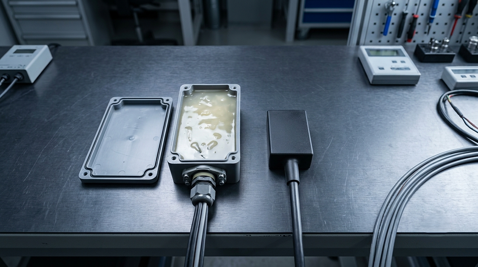
Overmolding differs from the traditional resin potting technique. Conventional potting requires maintaining an external shell that serves as a receptacle for pouring liquid resin. This process is characterized by very long chemical curing times, complex handling of reactive substances, and significant weight.
Conversely, direct overmolding eliminates the need for this container by injecting the polymer into the cavities of a temporary metal mold, generating a finished, watertight part that is immediately ready for handling upon ejection. The entire process is reduced to just three physical steps, compared to seven to eight manual steps for traditional coating.
The advantages of eliminating the casings
Volumetric reduction and structural integration
Eliminating the physical casing significantly reduces the overall assembly size. The outer shell thickness can be optimized to as low as 1.5 mm nominal thickness, eliminating the weight associated with mechanical fasteners, screws, spacers, and clips. This results in a final product with maximized compactness, essential for integrating dense embedded systems or lightweight portable devices.
Continuous sealing and mechanical resistance
By continuously encasing the components and wire connections, overmolding creates a watertight barrier against the ingress of foreign matter. High protection ratings such as IP67, IP68, and IP69 can be achieved, providing protection against prolonged immersion under pressure and intensive cleaning.
Furthermore, the process allows for direct overmolding of cable exit points, natively incorporating strain reliefs that protect internal conductors from mechanical pull-out and repeated vibrations. The overmolded polymer also acts as a mechanical damper, absorbing the energy of direct physical impacts.
Heat dissipation and dielectric insulation
One of the limitations of conventional cases is the thermal insulation caused by the stagnant internal air layer, which acts as an insulating barrier and overheats the power components. Overmolding completely eliminates this gaseous interface.
By using highly filled thermosetting resins (up to 70-80% by mass) with advanced mineral additives, the thermal conductivity of the overmolding polymer can be increased tenfold, from 0.4-0.6 W/m*K for a standard resin to over 10 W/m*K. This high conductivity allows the outer shell to actively act as a heat sink. This eliminates the need for bulky metal heat sinks and thermal greases, while maintaining a high dielectric strength of 40-60 kV/mm to ensure electrical insulation.
Intellectual property protection
Encapsulating the electronics in a solid polymer matrix that bonds tightly to the components creates a physical barrier against reverse engineering and industrial espionage. Unlike a screwed-on package that a third party can disassemble to analyze the printed circuit board, an overmolded assembly cannot be disassembled non-destructively. Any attempt to mechanically or chemically extract the solid casing results in the instantaneous physical destruction of the bare chips, copper traces and surface components, preventing physical access to the hardware ( anti-tampering ).
Ecological sustainability
The transition to direct overmolding promotes responsible manufacturing practices. Hot-melt thermoplastics used in LPM, such as polyamides, are 100% recyclable. Injection sprues and feed channels can be ground, melted, and reintroduced into the production process, thus creating a zero-waste model and reducing the overall carbon footprint of electronic devices.
Key points: Recommendations for electronics designers
Direct overmolding represents a change that redefines the standards of miniaturization and protection of electronic equipment by replacing housings with a polymer shell. This process combines in a single manufacturing step environmental sealing (up to IP 69), shock absorption, heat dissipation and intellectual property protection. The transition to direct overmolding thus represents an accessible opportunity to optimize the reliability and compactness of various technological creations.


Comments